
📚 Hardware Acceleration
This note turns the hardware-acceleration lecture into a practical mental model. The recurring idea is simple: arithmetic is cheap only when the data needed for it arrives quickly. Most optimizations below improve either the work per instruction, the amount of simultaneous work, or the reuse of values already brought close to the processor.
I. Introduction and Motivation
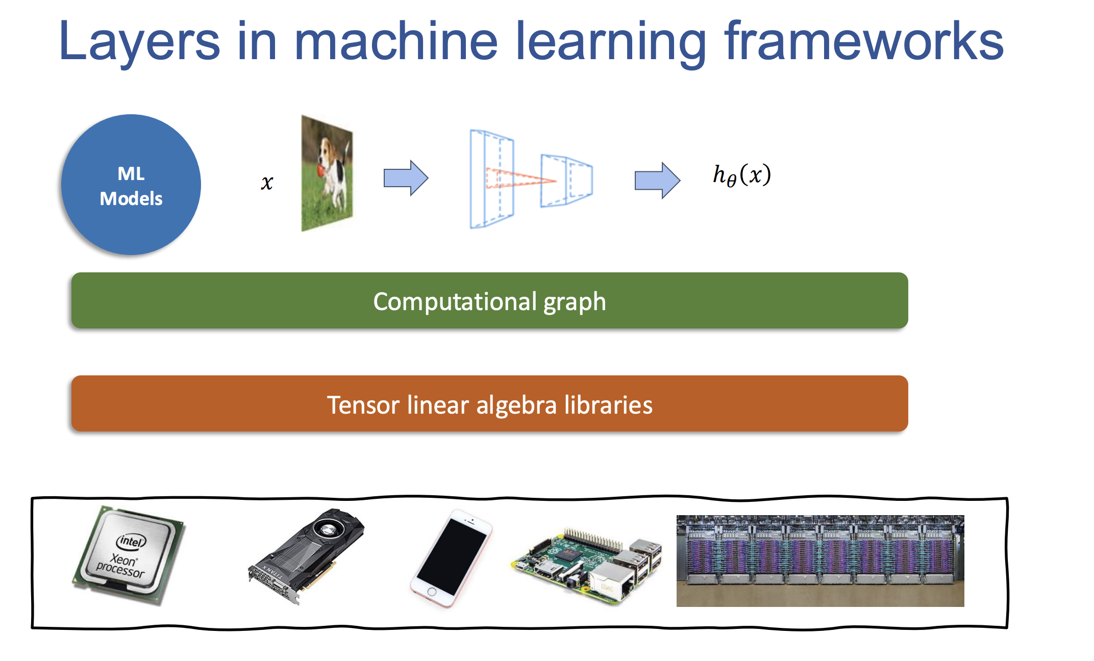
A deep-learning framework starts with tensor programs and computational graphs, then lowers them through tensor libraries and kernels to CPU or GPU instructions. A custom operator is useful only when it respects the hardware underneath it: arithmetic units, vector width, parallel workers, and memory hierarchy.
⚡ Necessity of Acceleration
Large models make both arithmetic throughput and memory movement important. Acceleration is the discipline of mapping tensor programs to the available CPU/GPU hardware so that it spends less time waiting for data and more time computing.
🛠️ Understanding Low-Level Details
The purpose is not to hand-write every low-level kernel. It is to recognize why high-level tensor code is fast or slow, how its layouts and loops become instructions, and where a custom operator would need a different strategy.
🧩 Custom Operator Implementation
When an operation is missing or unusual, the same questions guide its implementation: what is the parallel unit, what data can be reused, and which memory level should hold its working set?
II. Layers in Machine Learning Frameworks
🏗️ Hierarchical Structure
ML frameworks move from computational graphs, through tensor linear-algebra libraries, to device-specific kernels and hardware instructions. Each lower layer has more performance control and more implementation responsibility.
🔢 Tensor Linear Algebra
Tensor libraries present convenient multidimensional arrays and operations such as addition and matrix multiplication. Their implementations must account for shape, layout, dtype, and the device.
🔧 Need for Optimization
The same tensor operation needs a different implementation strategy on CPUs, GPUs, and mobile hardware. The rest of this post develops the CPU-oriented techniques that make that distinction concrete.
III. General Acceleration Techniques
Before looking at matrix multiplication, keep these ideas separate:
- SIMD vectorization: one CPU instruction processes several adjacent values.
- Thread parallelism: independent work is assigned to several CPU cores.
- Tiling / blocking: a small working set remains in faster memory and is reused.
They are complementary, but not synonyms. A float4 instruction does not create four CPU threads, and CPU cache tiling is not the same thing as CUDA shared-memory tiling.
📊 Vectorization: one instruction, several numbers
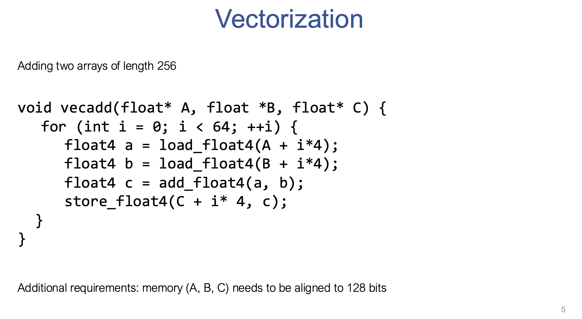
Modern CPUs have vector registers and vector instructions. Instead of adding one float at a time, a vector instruction can add several adjacent floats at once. The exact width depends on the CPU and instruction set.
How to read the slide
The slide adds arrays with 256 floats. float4 means a four-float, 128-bit vector:
for (int i = 0; i < 64; ++i) {
  float4 a = load_float4(A + i * 4);
  float4 b = load_float4(B + i * 4);
  float4 c = add_float4(a, b);
  store_float4(C + i * 4, c);
}
At i = 0, it processes elements 0 through 3. At i = 1, it processes 4 through 7. At i = 63, it processes 252 through 255. The 64 loop iterations cover all 256 floats because each iteration handles four values:
scalar version:  256 iterations × 1 float
vector version:   64 iterations × 4 floats
This is data parallelism inside one core. A compiler may generate the vector instructions automatically, or a library/kernel can use intrinsics explicitly.
Concrete value-level example
If the first four values are:
A[0..3] = [1, 2, 3, 4]
B[0..3] = [10, 20, 30, 40]
then the first vector iteration behaves like four scalar additions bundled into one vector operation:
load a = [1, 2, 3, 4]
load b = [10, 20, 30, 40]
add    = [11, 22, 33, 44]
store C[0..3] = [11, 22, 33, 44]
If the array length is not divisible by the vector width, a real kernel also needs a short scalar tail or a masked vector operation for the final one to three elements.
Why contiguous layout and alignment matter
The four floats should be consecutive in memory, so a vector load can fetch one 16-byte range:
A + 0 bytes:  [A0 A1 A2 A3]   one aligned float4 load
A + 16 bytes: [A4 A5 A6 A7]   next aligned float4 load
Four floats occupy 16 bytes = 128 bits. The slide’s alignment requirement means the base address and relevant offset should be compatible with that 16-byte access. An unaligned or non-contiguous input may still work on modern hardware, but can require extra instructions or prevent clean vectorization.
The key distinction:
- Vectorization uses adjacent data within one instruction.
- CPU threading uses multiple cores at the same time.
- GPU warps execute 32 GPU threads in lockstep; that is a different hardware model.
🗂️ Data Layout and Strides
An array is ultimately a one-dimensional allocation. Its shape tells us how we view that allocation; its strides tell us how far to move in memory when an index changes.
Consider a row-major 3 × 4 matrix:
logical matrix                         underlying buffer

[[ 0,  1,  2,  3],                    [0, 1, 2, 3, 4, 5,
 [ 4,  5,  6,  7],                     6, 7, 8, 9, 10, 11]
 [ 8,  9, 10, 11]]
Its shape is (3, 4) and its element strides are (4, 1):
offset(row, col) = row × 4 + col × 1

x[2, 3] lives at offset 2 × 4 + 3 = 11
The first stride, 4, means “move four floats to advance by one row.” The second stride, 1, means “move one float to advance by one column.” In a column-major matrix the same shape would commonly have strides (1, 3).
A transpose is often a view, not a copy
Transposing the matrix can change only metadata:
x:       shape (3, 4), strides (4, 1)
x.T:     shape (4, 3), strides (1, 4)

x.T[3, 2] -> offset 3 × 1 + 2 × 4 = 11 -> value 11
No values need to move. The same buffer is interpreted with a new shape and stride pair. This is why transpose, slicing, and reshaping can be inexpensive views.
Strided views have a cost
Take every other column:
x[:, ::2] has shape (3, 2), strides (4, 2)

[[0, 2],
 [4, 6],
 [8, 10]]
This is still zero-copy, but consecutive logical elements now sit two floats apart. A vector unit and cache prefer contiguous runs of data. Frameworks often make a contiguous copy before an operation whose kernel requires contiguous input. A stride is not inherently bad; it trades avoiding a copy now for giving a later kernel an awkward access pattern.
Reading a 2D stride as an address calculation
For an array with shape (3, 4) and strides (4, 1), indexing x[1, 2] means:
start at the base
move 1 row  ->  1 × 4 elements
move 2 cols ->  2 × 1 elements
total offset = 6, so x[1, 2] = 6
For the transpose view x.T, the same value is written x.T[2, 1]. Its strides are (1, 4), so the address is still offset 2 × 1 + 1 × 4 = 6. This is the essential point: a transpose view changes the mapping from indices to addresses, not the underlying values.
🧵 Parallelization: independent outputs, independent workers
Vectorization divides one instruction into lanes. Parallelization divides a program into work items that can run on different cores. The first question is always: does each work item write to a distinct result, or is there safe synchronization?
For elementwise addition, each output index is independent:
#pragma omp parallel for
for (int i = 0; i < n; ++i) {
  C[i] = A[i] + B[i];
}
The OpenMP directive asks the runtime to distribute iterations across CPU threads. It is safe because no two iterations write the same C[i].
For a reduction, all iterations contribute to one number. This needs a reduction clause rather than unsynchronized updates:
float sum = 0.0f;
#pragma omp parallel for reduction(+:sum)
for (int i = 0; i < n; ++i) {
  sum += x[i];
}
For matrix multiplication, one useful mapping gives one worker ownership of one output element, or a small output tile. Each worker keeps its accumulator private until it writes its distinct result. This avoids races and is the bridge to the tiled examples below.
Example: safe and unsafe accumulation
Suppose two workers both execute an unsynchronized sum update. Each update is read, add, write—not one indivisible action. Both workers can read the same old sum and one update can overwrite the other. The reduction clause gives each worker a private partial sum and combines those partial sums safely at the end.
For a matrix, this ownership is natural:
worker 0 owns C[0, 0] and its private accumulator
worker 1 owns C[0, 1] and its private accumulator
...
each worker writes its result once after completing K
The same idea scales from one output element to a register tile such as a 2 × 3 block of C.
IV. Case Study: Matrix Multiplication
✏️ Vanilla Implementation
The lecture slides use a row-dot-row convention:
C = A × Bᵀ
C[i, j] = sum over k of A[i, k] × B[j, k]
This is equivalent to the usual A × B formulation except that B is stored/transposed differently. It matters because the slide code accesses B[j][k]: it takes row j of B, not column j.
For two 2 × 2 matrices:
A = [[a00, a01],       B = [[b00, b01],
     [a10, a11]]            [b10, b11]]

C = A × Bᵀ
C00 = a00×b00 + a01×b01
C01 = a00×b10 + a01×b11
for (int i = 0; i < n; ++i) {
  for (int j = 0; j < n; ++j) {
    float acc = 0.0f;
    for (int k = 0; k < n; ++k) {
      acc += A[i][k] * B[j][k];
    }
    C[i][j] = acc;
  }
}
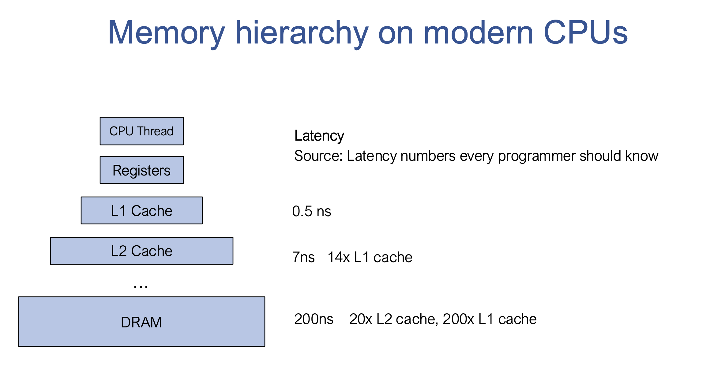
It performs roughly n³ multiply-adds. The arithmetic is not the whole story: it repeatedly needs values from A and B. The hierarchy is broadly:
DRAM  ->  L2 cache  ->  L1 cache  ->  registers
large, slow                               tiny, fastest
🧱 Memory Hierarchy Importance
Registers are the smallest and fastest storage, followed by L1/L2 caches, then DRAM. The precise latency varies by machine, but the order matters: moving a reused value once is far cheaper than repeatedly waiting for it from a lower level.
🏗️ Architecture Aware Analysis
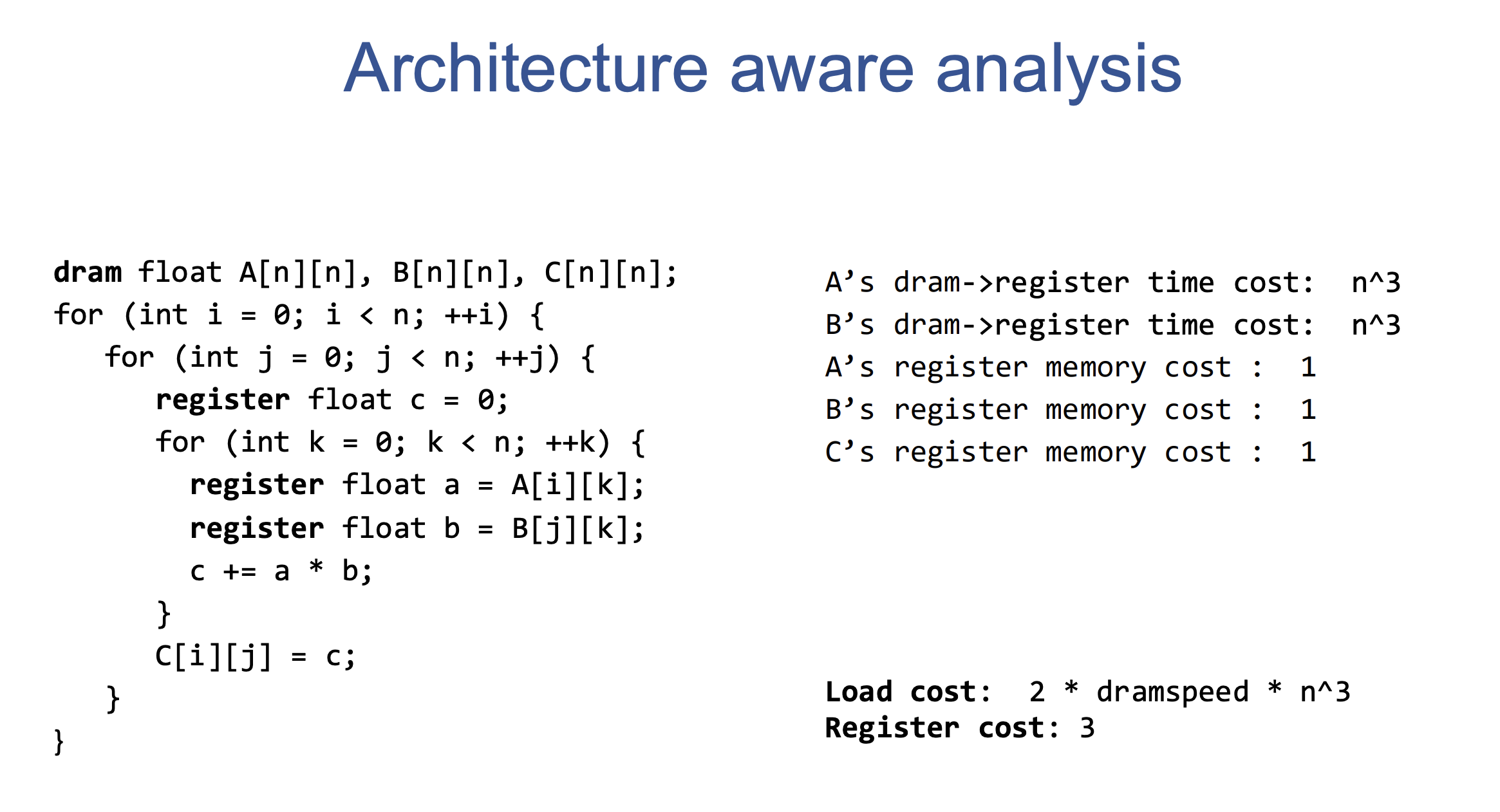
The slide is a deliberately simplified model: every inner-loop read of A[i][k] and B[j][k] is charged as a DRAM-to-register load. That yields about n³ loads of each input. Real CPUs cache automatically, so this is not a literal timing prediction; it exposes the opportunity to reuse one load for several arithmetic operations.
For example, in the naïve loop, computing C[0, 0] reads A[0, 0], A[0, 1], and so on. Computing C[0, 1] immediately afterwards needs the same row of A again. A tiled algorithm tries to keep a fragment of that A row close by while both outputs are computed.
🧮 Register Tiled Implementation
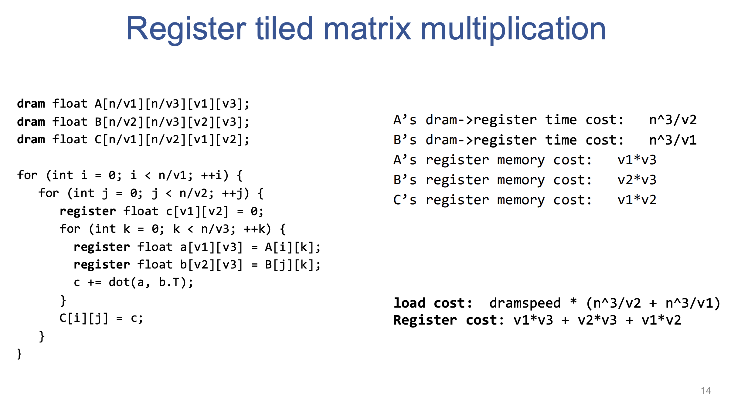
The v1, v2, and v3 labels on the slide describe one small multiplication phase:
A panel: v1 × v3 B panel: v2 × v3 C tile: v1 × v2
Because this article uses C = A × Bᵀ, the B panel has v2 rows. Its transpose is conceptually v3 × v2, so multiplying the panels produces a v1 × v2 output tile.
for (int I = 0; I < n; I += v1) {
  for (int J = 0; J < n; J += v2) {
    float c[v1][v2] = {0};             // registers: one output tile

    for (int K = 0; K < n; K += v3) {
      float a[v1][v3] = load(A[I:I+v1, K:K+v3]);
      float b[v2][v3] = load(B[J:J+v2, K:K+v3]);
      c += a × transpose(b);           // outer-product-like tile update
    }

    store(C[I:I+v1, J:J+v2], c);
  }
}
The notation above is pseudocode: the slices express which data is loaded, not a particular C syntax.
Worked 2 × 3 × 1 example
Set v1 = 2, v2 = 3, v3 = 1. In one K phase, the kernel loads:
a = [[a00],            b = [[b00],
     [a10]]                 [b10],
                           [b20]]
Then it updates all six accumulators of a 2 × 3 C tile:
[[c00, c01, c02],      += [[a00×b00, a00×b10, a00×b20],
 [c10, c11, c12]]          [a10×b00, a10×b10, a10×b20]]
This is the key reuse:
- one loaded a00 contributes to three output columns;
- one loaded b00 contributes to two output rows;
- the six c partial sums stay in registers across the K loop.
On the next K phase, a and b are overwritten with the next K slice, while the c accumulators remain. Values from an earlier K slice are not needed again after their contributions to the current C tile have been made.
Two K phases, step by step
To see why the old A values are not needed after a phase, take a 2 × 4 A panel and three 1 × 4 B rows. Use K tiles of width 2:
A = [[a00, a01 | a02, a03],
     [a10, a11 | a12, a13]]

B = [[b00, b01 | b02, b03],
     [b10, b11 | b12, b13],
     [b20, b21 | b22, b23]]
The first K phase loads the left halves. All six C accumulators are updated before those values are discarded:
C00 += a00×b00 + a01×b01     C01 += a00×b10 + a01×b11
C02 += a00×b20 + a01×b21
C10 += a10×b00 + a11×b01     C11 += a10×b10 + a11×b11
C12 += a10×b20 + a11×b21
The second K phase overwrites the A and B registers with the right halves and adds the remaining products:
C00 += a02×b02 + a03×b03     C01 += a02×b12 + a03×b13
C02 += a02×b22 + a03×b23
C10 += a12×b02 + a13×b03     C11 += a12×b12 + a13×b13
C12 += a12×b22 + a13×b23
After phase one, a00 and a01 have already contributed to every output in this 2 × 3 C tile that needs them. Keeping them would not help phase two; the accumulators C00 through C12 are the values that must survive.
The slide’s simplified load counts summarize this reuse:
A loads: about n³ / v2       each A value is reused across v2 output columns
B loads: about n³ / v1       each B value is reused across v1 output rows
Larger tiles improve reuse but consume more registers. Too many registers can reduce how many independent instructions or threads the processor can keep active, so tile size is an engineering trade-off, not “as large as possible.”
🗄️ Cache Line Aware Tiling
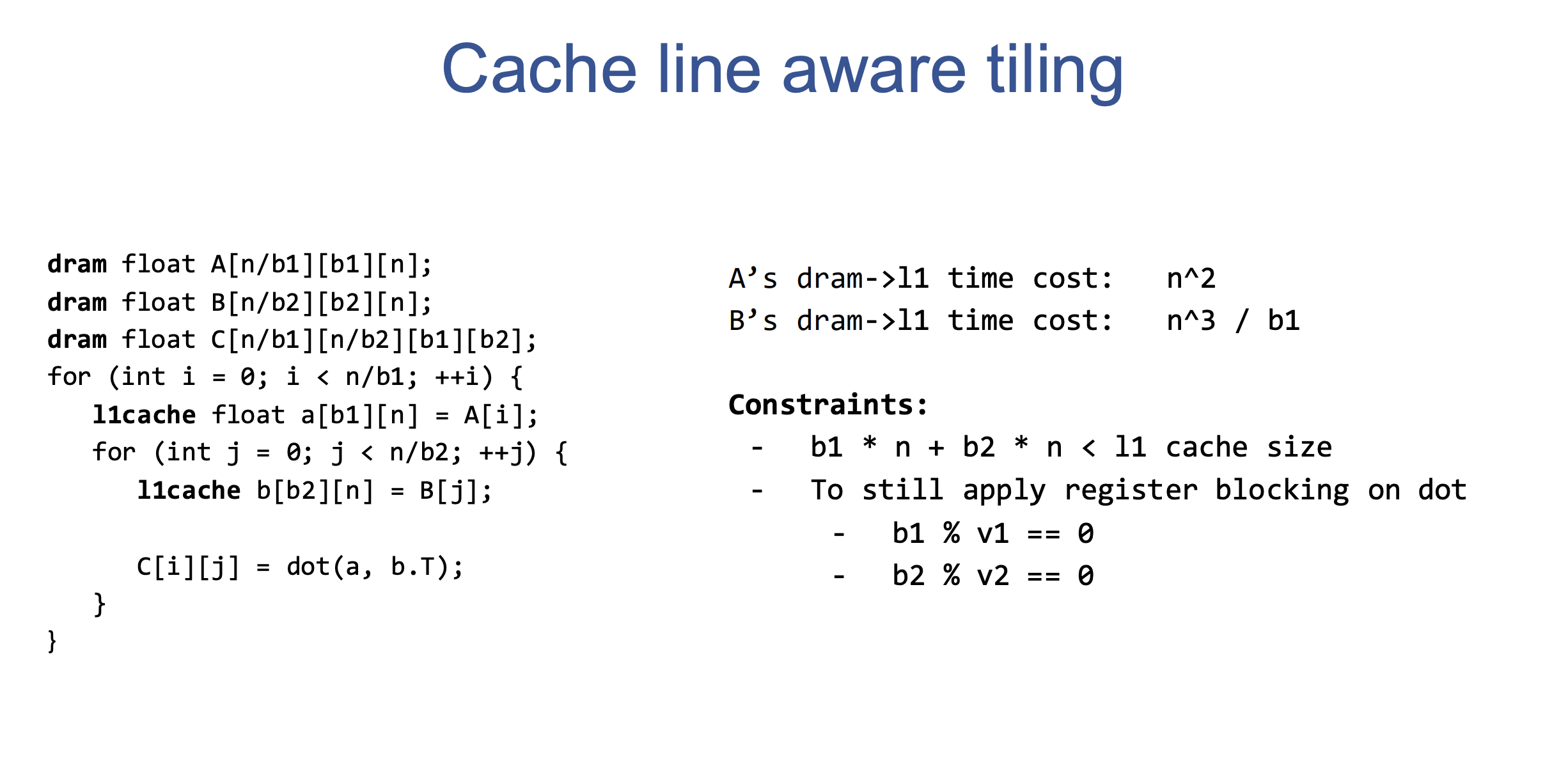
Registers are too small for a large matrix panel. CPUs therefore add a second level of blocking that works with L1 cache. The CPU cache is hardware-managed: source code requests a normal load, and the cache controller brings cache lines into L1 when possible. A cache tile is a loop order and working-set choice that makes those automatic cache hits likely.
The slide uses:
b1 × n panel of A       b2 × n panel of B       cache-level C block: b1 × b2
v1 × v2 register tile inside that cache block
At a high level:
for (int I = 0; I < n; I += b1) {          // cache-sized A panel
  for (int J = 0; J < n; J += b2) {        // cache-sized B panel
    for (int i = I; i < I + b1; i += v1) { // register tiles
      for (int j = J; j < J + b2; j += v2) {
        compute_register_tile(i, j);
      }
    }
  }
}
The factors b1 and b2 must be large enough to create reuse, but small enough that useful A and B panels fit alongside other live data in L1. In the lecture’s simplified accounting:
DRAM -> L1:
  A panel work costs about n²
  B panel work costs about n³ / b1

L1 -> registers:
  A work costs about n³ / v2
  B work costs about n³ / v1
These are asymptotic movement counts, not exact latency formulas. Their lesson is which loop direction enables reuse. Holding an A panel while moving across J lets it serve many B panels; holding a register A fragment while producing v2 output columns lets it serve several multiply-adds.
A concrete cache and register choice
Imagine choosing b1 = 4 and b2 = 8 for a cache-level C block, then v1 = 2 and v2 = 4 for each register tile. One cache block covers a 4 × 8 region of C. It contains four 2 × 4 register tiles:
C cache block (4 × 8)

[ register tile 0 | register tile 1 ]
[ register tile 2 | register tile 3 ]
The A panel for those four tiles is retained while the algorithm moves across the two groups of output columns. Each small register tile then loads only the A/B fragments it needs for its own accumulators. The cache level creates reuse across several register tiles; the register level creates reuse across several multiply-adds inside one tile.
🧩 Putting it All Together
🔄 Multi-Level Tiling
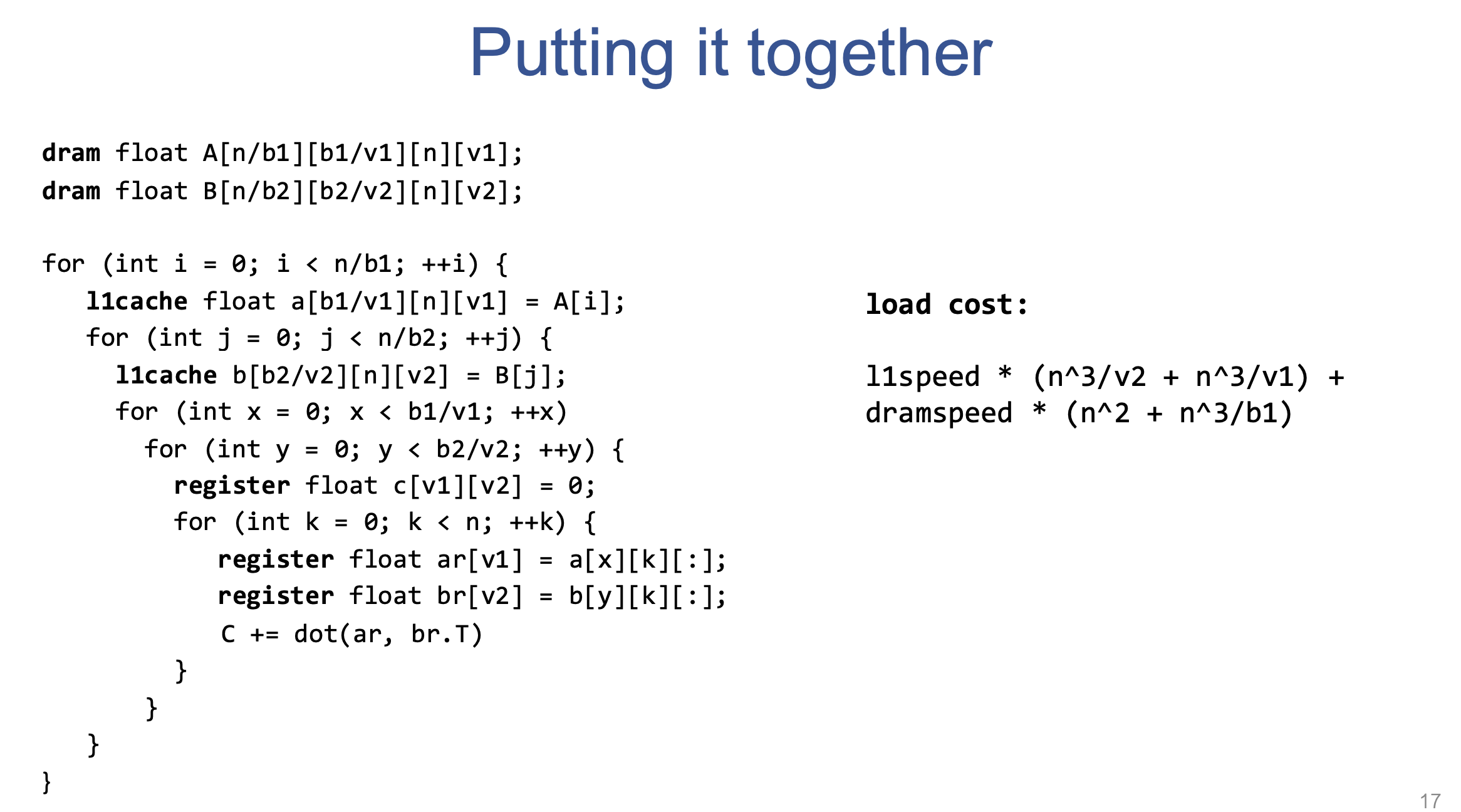
The final slide combines the two levels:
- choose cache blocks (b1, b2) that fit in the L1 working set;
- within a cache block, choose small register tiles (v1, v2);
- retain the output tile accumulators in registers through its K loop;
- write the completed output tile once.
The diagram’s nested loops are ownership and reuse scopes:
outer I/J cache block:        reuse data while it stays cache-resident
inner i/j register tile:      reuse fragments while they stay in registers
inner K accumulation loop:    add every K contribution to the same C tile
This is a CPU-oriented model. On a GPU, the analogous discussion adds blocks, warps, global memory, and explicit shared memory; the central principle is still data reuse, but the programmer controls different pieces of the hierarchy.
The full nesting in one sentence
For one cache-sized C block, hold the useful A/B panels in cache; for one small C tile inside it, hold partial sums and tiny A/B fragments in registers; then walk along K until that output tile is complete. The work becomes efficient because each memory level supplies a value to several calculations before it is replaced.
💡 Key Insight: Memory Load Reuse
Across all of these variations, loop tiling isolates a scope in which a value can be loaded once and used several times. Register tiles create the shortest reuse scope; cache tiles create a larger one around several register tiles.
V. Conclusion
🔍 Summary of Techniques
When a tensor operation is unexpectedly slow, work through these questions:
- Is the data contiguous, or do strides force scattered accesses?
- Can the compiler/library vectorize the inner loop?
- Are iterations independent enough to run in parallel without races?
- Is a value reloaded from a slow level when a tile could reuse it?
- Does a larger tile exceed the cache/register budget and make things worse?
📈 Hardware Awareness
Hardware-aware programming means matching an implementation to the layout, instruction width, parallel workers, and memory hierarchy of the target device. It is not merely reducing operation count.
🔁 Reuse Principle
The goal is not to manually write every kernel. It is to recognize why high-performance libraries choose a particular layout, loop order, vector width, and tiling strategy—and to have a disciplined way to reason about an operator when its performance surprises you.